Scanning Electron Microscopy Laboratory
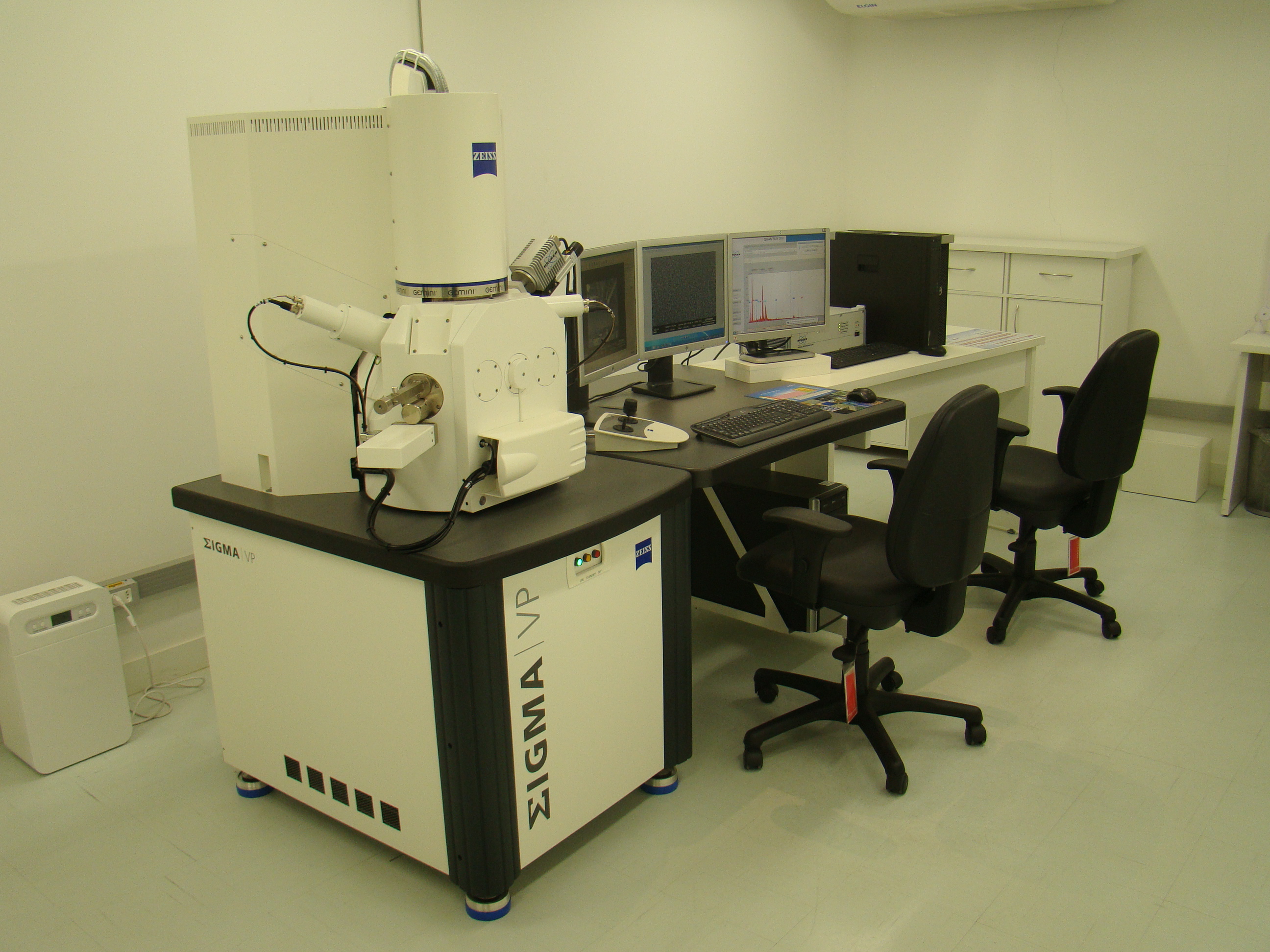
The CDTN Electron Microscopy Laboratory is comprised of a field-effect emission scanning electron microscope (FEG-MEV), model SIGMA VP, manufactured by Carl Zeiss Microscopy. The equipment operates in high vacuum and variable pressure (VP) modes. In VP mode, it is possible to obtain images of materials that are not electrically conductive, without the need to apply conductive coatings. A distinguishing feature of the microscope is the GEMINI® column, whose design allows for excellent image quality even when operating at low voltages.
The equipment has four detectors, three of which are secondary electron detectors (two for high vacuum and one for variable pressure) for obtaining images based on topographic contrast, and one backscattered electron detector for images obtained based on atomic number contrast.
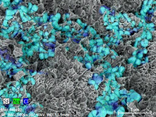
The microscope also has a microanalysis system consisting of an energy dispersive X-ray spectrometer (EDS), model XFlash 410-M, supplied by Bruker Nano GmbH. The system is controlled by ESPRIT software and is capable of performing spot analyses, line scans and obtaining element distribution maps.
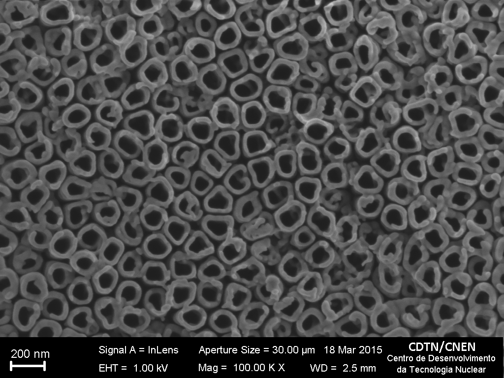
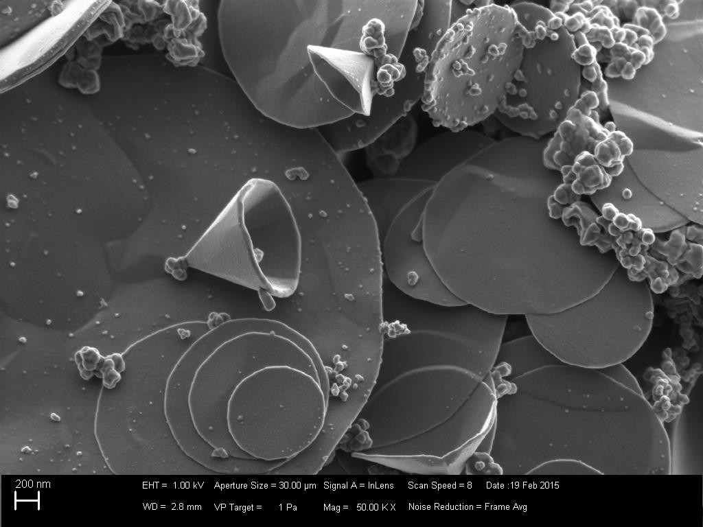
The equipment can analyze metallic samples, minerals, magnetic materials, polymers, carbon nanotubes, biocompatible materials and ceramics, with structures on the nanometric scale.
The factory technical specifications of the FEG-MEV SIGMA VP are listed in the Table below.
|
Resolution |
1,3 nm a 20 kV 1,5 nm a 15 kV 2.8 nm a 1 kV 2,5 nm a 30 kV, no modo VP |
|
Acceleration voltage |
0,1 – 30 kV |
|
Current in sample |
4 pA a 20 nA |
|
Magnification |
12x – 1.000.000x |
|
Electron emitter |
Thermal Schottky field emission |
Contact
Advanced Materials Multi-User Unit - agendamentos.granioter@cdtn.br - Tel: +55 31 3439-9394